Prototyping for Photonics
Yi Zhang, Yang Liu, Tom Baehr-Jones and Michael Hochberg
Electrical Engineering, University of Washington
(Nanophotonics Lab Website / OPSIS website)
In support of the OPSIS silicon photonics foundry program, the Nanophotonics Group has used the e-beam system to build prototype devices to study design parameters. Data from these explorations have guided device design in the larger-scale integrated systems built in the Opsis program.
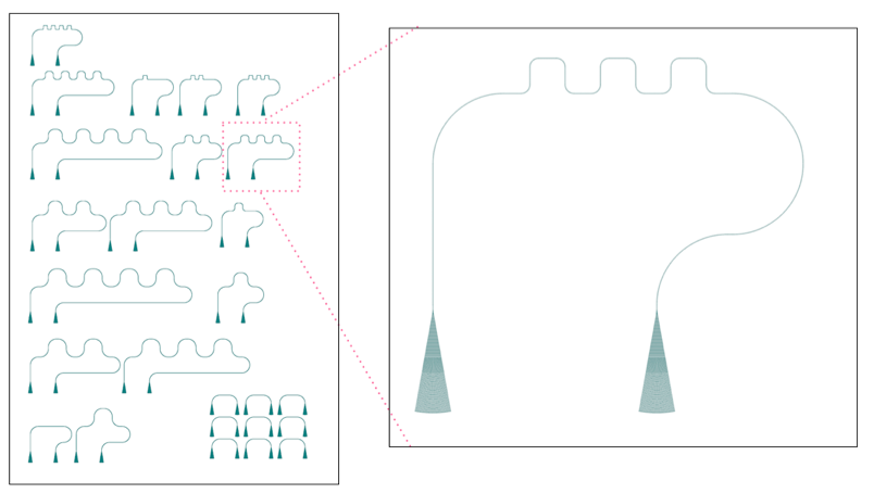
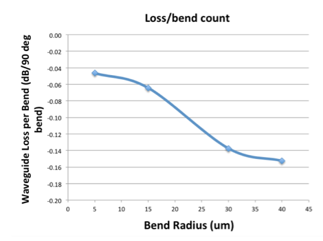
Example: Waveguide Bend Radius
To optimize design for more complex devices, it is necessary to understand loss around corners of varying bend radius. In a quick experiment, the design shown here varies bend radius and number of bends to provide quick feedback on the bend radius / waveguide loss tradeoff.
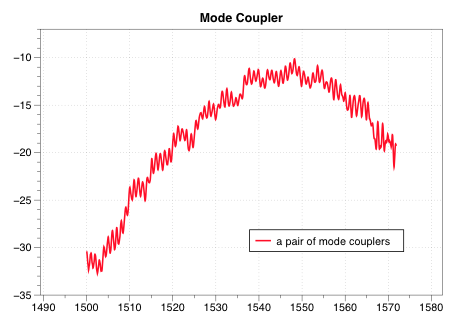
Example: Verification of a Mode Coupler Design
Complex systems require light to travel in both ridge and slot waveguides; the transition from one type to the other always introduces some loss to the light propagation. It is desirable to minimize this transition loss. In this example, a test chip was built which allowed a large matrix of design parameters to be evaluated, thus validating the FDTD simulations for these couplers.
Example design for a tapered mode coupler to couple light from a ridge waveguide (bottom) to a slot waveguide (top).

A sweep of loss versus wavelength for a pair of mode couplers - light is coupled from a ridge waveguide to a slot waveguide and then back to a ridge waveguide.
Measurement summary showing loss plotted against the number of couplers, for both 100 nm and 80 nm slot waveguides.
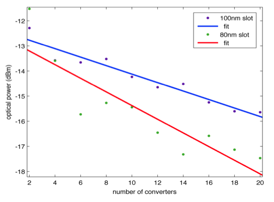
Results:
- 500 nm ridge w/ 100 nm slot: 0.17 +/- 0.02 dB/coupler
- 500 nm ridge w/ 80 nm slot: 0.27 +/- 0.06 dB/coupler
- No strong wavelength dependence observed
These results show exceptionally low-loss coupling from the ridge waveguide into a slot waveguide. This optimal design is now used in complex Opsis system designs.