Optical Trapping in a Photonic Crystal Microcavity: Chip Based Cavity QED
Hamed Mirsadeghi and Jeff Young, Dept of Physics and Astronomy, University of British Columbia, Vancouver, Canada
Photonics and Nanostructures Laboratory Website
The objective of this project is to study the interaction of single metal and semiconductor nanoparticles with single photons: cavity quantum electrodynamics. This is to be done on a wafer-scale, using silicon-on-insulator optical circuits to excite and probe the interaction region, defined by a photonic-crystal-based optical microcavity. The microcavity is based on a slot-waveguide geometry which supports mode’s localized primarily outside of the silicon. By operating the circuit in a solvent (such as hexane), containing metal and/or semiconductor nanocrystals, efficient optical trapping of the nanoparticles at the antinode of the cavity is expected.
After simulating and optimizing the photonic device using Finite Difference Time Domain (FDTD) method, the designs were fabricated at the UW Microfabrication Facility. The initial tests on the chip have been done and the transmission through the slot-cavity was measured and compared with simulation results in the figure below. The results show very good agreement between simulation and experiment.
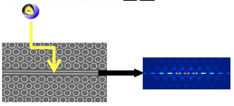
Figure 1: Experimental Diagram: Nanoparticle will be “self-aligned” in cavity via optical trapping.
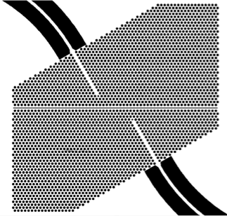
Figure 2: Layout, holes represent photonic crystal and lines represent 1D defects (grating couplers not shown).
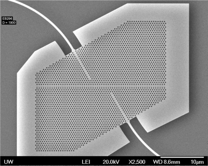
Figure 3: SEM micrograph of the fabricated photonic crystal microcavity.
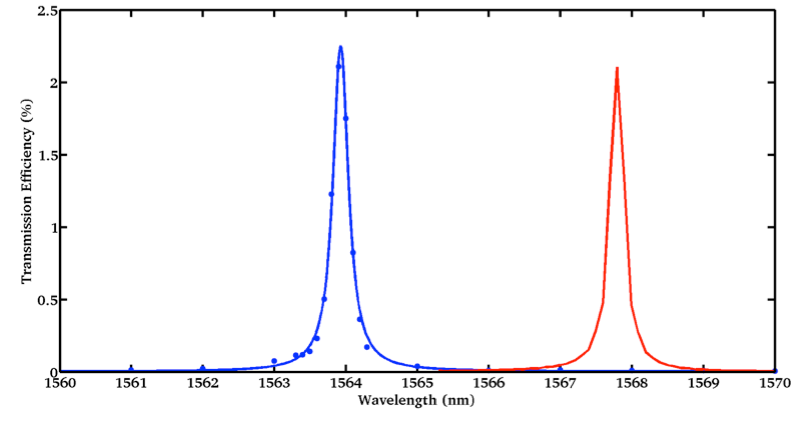
Figure 4: Resonant transmission spectra from input to output ridge waveguides through slot-cavity in hexane solvent. The simulation curve is red (right curve) and the experimental data points, fitted with a Fano line-shape are plotted in blue (left curve).
Beside the main objective of this project, which is trapping nanoparticles, these devices can be used as fluid refractive index sensor. The resonance of the cavity, which is the wavelength of the transmission peak, shifts upon changing the refractive index medium. The fabricated cavities, showed sensitivity of 370 nm per unit of refractive index change.
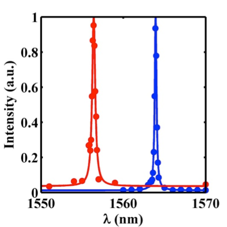
Figure 5: Resonant transmission spectra for two different devices in hexane (blue,on the right) with refractive index of 1.365 and acetone (red, on the left) with refractive index of 1.346.
Publications:
S.Hamed Mirsadeghi, Ellen Schelew, Jeff F. Young, “Photonic crystal slot-microcavity circuit implemented in silicon-on-insulator: High Q operation in solvent without undercutting,” Applied Physics Letters, 102, Page 131115 (2013). doi: 10.1063/1.4799963
S.Hamed Mirsadeghi, Ellen Schelew, Jeff F. Young, “Optical Sensing and Trapping in Photonic Crystal Slot Cavities,” 17th PCAMM Annual Meeting (2012) Poster Presentation.
S.Hamed Mirsadeghi, Jeff F. Young, “ Optical Trapping in Silicon-Based Photonic Microcavities,” 14th Annual Meeting of the Northwest Section of the APS (2012) Poster Presentation.