Graphene Optoelectronics
Jason S Ross, Xiaodong Xu
Dept of Physics, University of Washington
(Nanoscale Optoelectronics Laboratory Website)
The remarkable physical properties of graphene and nanotubes make them perfect candidates for new classes of optoelectronic and spintronics devices. Graphene is a two-dimensional membrane formed by carbon atoms in a hexagonal structure. Although it is only one atom thin, it can universally absorb a remarkable 2.3% of light from the visible to infrared range, which ranks graphene as one of the materials with the strongest interband transition. Graphene’s electronic structure can be controlled by its size and shape, applied electrical field, and chemical modifications. With its extremely high electron mobility, graphene is an extraordinary material for engineering fully-integrated, high-speed and flexible optoelectronics carved from single graphene sheets.
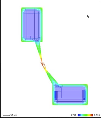
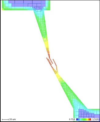
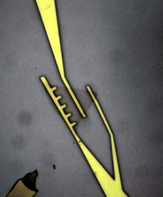
For this work, electron-beam lithography is used to define contacts which are custom-designed and carefully aligned to each monolayer graphene flake on a substrate. Proximity Effect Correction is used to ensure accurate shape fidelity over a wide range of designs, with the exposure dose being modulated by more than a factor of 2 between the large contact pads and the fine features atop the graphene.
Publications:
Ultrafast hot-carrier-dominated photocurrent in graphene. Dong Sun, Grant Aivazian, Aaron M. Jones, Jason S. Ross, Wang Yao, David Cobden and Xiaodong Xu. Nature Nanotechnology, 15 Jan 2012.