Silicon Nanowires
Golam Rabbani, M.P. Anantram
Electrical Engineering, University of Washington
The group investigates the transport physics and optical properties of silicon nanowires. Theory predicts that a Silicon Nanowire narrow enough and under direct strain will behave as a direct-gap semiconductor, which would find use as a good optoelectronic component. Using the JEOL ebeam system, followed by etching, the group has fabricated a variety of sizes of wires smaller than 50 nm wide.
Image of a 40 nm wide silicon nanowire etched into silicon.
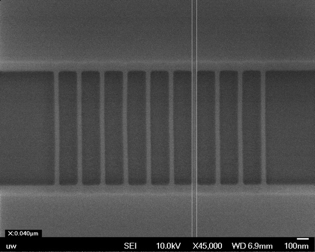
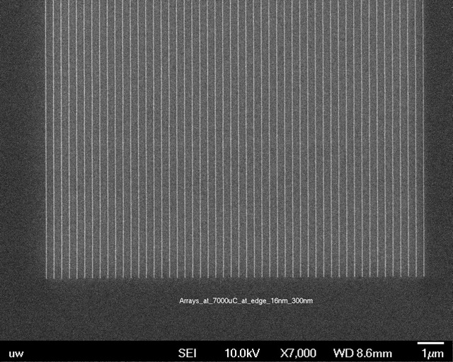
An array of nanowires in resist.
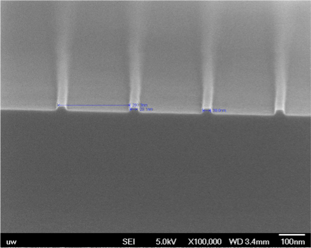
A cross-section SEM image of silicon nanowires, 30 nm wide.
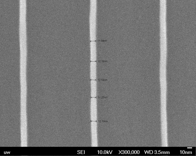
12 nm wide nanowires imaged in HSQ e-beam resist. Future work will improve the etching process to transfer this pattern into the underlying silicon.